
 News
News Industry News
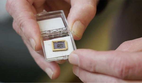
Although graphene has the potential to improve the efficiency and performance of electronic products, material mimics have prevented anyone from transforming its potential into functional semiconductors - until now. In groundbreaking research at the Georgia Institute of Technology, scientists created the world's first successful graphene semiconductor.

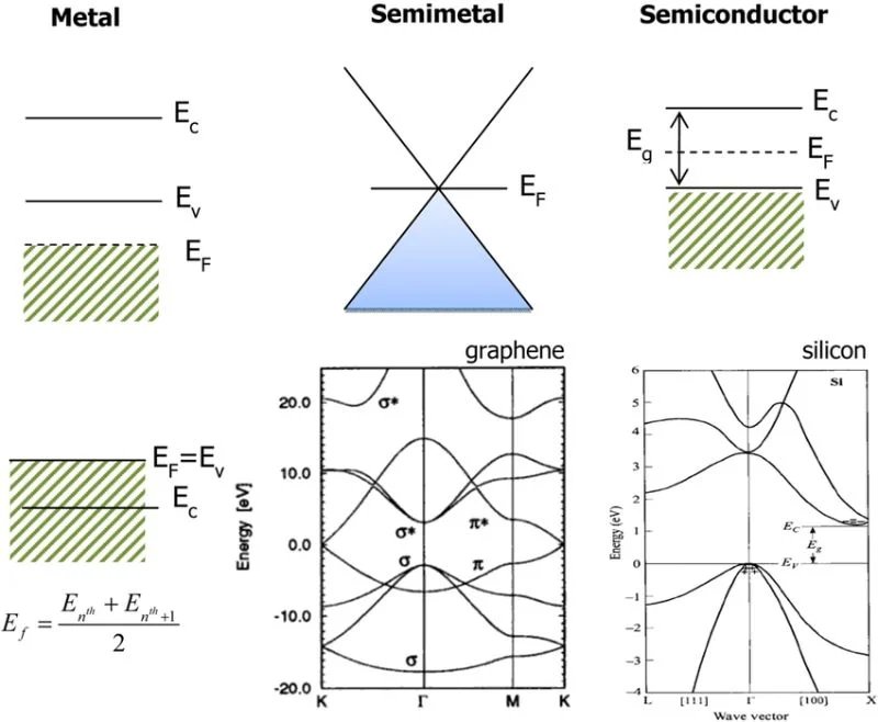
Graphene: A Semi Metal
Graphene has long been considered a material with excellent electrical properties, including high electron mobility, excellent thermal conductivity, and excellent mechanical strength. The single-layer structure of its carbon atoms arranged in a two-dimensional honeycomb lattice allows electrons to pass through it with minimal resistance, making it one of the most conductive materials known.
However, despite its enormous potential, other phySICal limitations hinder its use in traditional semiconductor applications.
In its inherent state, graphene is classified as a semimetal, which means it naturally does not behave like a semiconductor or metal. In order for the material to effectively function in electronic devices such as transistors, it requires a bandgap so that the material can "turn on" and "turn off" through an electric field. This principle supports the functionality of silicon-based electronic devices. Therefore, the main challenge of using graphene for electronic applications is to induce this silicon like switchable property without compromising its inherent properties.
Research on Graphene at Georgia Institute of Technology
Recently, a research team from Georgia Institute of Technology claimed to have created the world's first graphene based semiconductor device.
Researchers have successfully demonstrated that well annealed apparent graphene on specific silicon carbide crystal faces can serve as a high mobility two-dimensional semiconductor. Specifically, the team developed semiconductor apparent graphene (SEG) on a single crystal silicon carbide substrate, with a bandgap of 0.6 eV and a room temperature mobility of over 5000 cm ²/ Vs is significantly higher than silicon and other two-dimensional semiconductors.

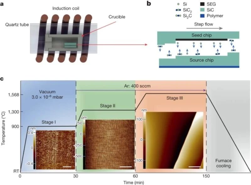
The production of SEG involves restricted control sublimation (CCS) furnaces, in which semi insulating SiC chips are annealed in a graphite crucible under an argon atmosphere. The temperature and rate of graphene formation are precisely controlled, with the escape rate of silicon from the crucible playing a crucial role.
To characterize SEG, the team used scanning tunneling microscopy (STM), scanning electron microscopy (SEM), low-energy electron diffraction (LEED), and Raman spectroscopy. These methods allow for detailed examination of SEGs at multiple scales, distinguishing them from bare SiC and graphene, and confirming their atomic alignment with SiC substrates.
The potential of semiconductor apparent graphene
The research team emphasized the potential of SEG in the field of nanoelectronics.

As a well crystallized two-dimensional semiconductor with significant bandgap and high mobility, SEG represents a significant step forward for the industry in achieving electrical advantages in materials such as graphene. Future work will focus on reliably producing large platforms with suitable dielectrics, managing Schottky barriers, and developing integrated circuit solutions. Ultimately, the research team believes that SEG has the potential for commercial feasibility and has a tangible impact on 2D nanoelectronics.