

 News
News Industry News
Infineon has released its second-generation CoolSIC mosfet devices with voltage levels of 650 V, 1200 V, and 3300 V, targeting high-voltage industrial applications such as electric vehicle charging, industrial solar inverters, servo drives, UPS, and railway traction. For low-voltage applications such as server power factor correction, multi-level solar topology, and high-power drivers, Infineon will launch a 400 V SiC MOSFET with a channel resistance range of 11 m Ω to 45 m Ω, using two different 4-pin packages - TOLL and D2PAK-7.
Industrial grade CoolSiC MOSFET 650 V discrete overview
Infineon's latest 650 V split MOSFET is based on second-generation (G2) SiC trench technology. The first generation (G1) CoolSiC grooves focus on providing reliable performance and achieving an industry-leading balance between performance and reliability - these features help win customer trust in the new SiC technology. On this basis, G2 has added better performance, greater flexibility in use, and advanced packaging technology, while maintaining the reliability and robustness of G1 relative to the gate oxide layer (GoX). The switching behavior of Infineon's second-generation SiC MOSFET is remarkable. The coefficient of performance (FOM) graph shown in Figure 1 highlights significant improvements compared to the previous generation.
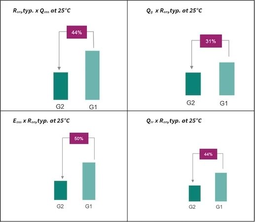
Figure 1
The strong FOM indicates that Infineon's G2 SiC MOSFET can successfully adapt to high-frequency designs, which is a typical feature of soft switching topologies. Overall, they can achieve higher system power density. It is interesting that the improvement in CoolSiC G2 switch performance balances the increase in thermal coefficient. Figure 2 shows the temperature dependence of Ron at 25C for different Infineon 650V power device technologies and generations. At 125C, the R on of CoolSiC G2 increased by 12% compared to G1. However, it is still at least 20% lower than CoolGaN G1 and CoolMOS 7.
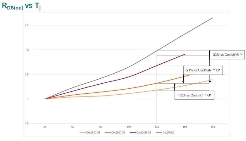
Figure 2
The device resistance has a stronger dependence on temperature, which will not affect the overall performance of CoolSiC MOSFET 650 V G2, especially during system level evaluation. System loss is usually the sum of conduction loss and switching loss. The conduction loss is mainly related to R on, but the switching loss depends on different parameters. The optimal switching behavior of CoolSiC MOSFET G2 helps to offset the more significant increase in Ron with temperature. It made G2 perform well, achieving a stable peak efficiency of 99.2% in the 3.3 kW continuous conduction mode totem (CCM) pole PFC measurement, as shown in Figure 3.
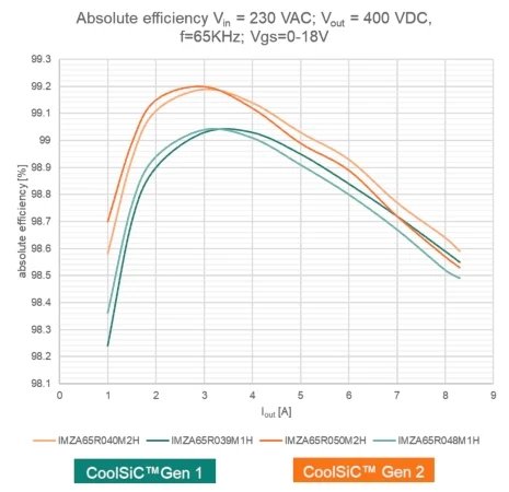
Figure 3
In addition to performance, CoolSiC G2 also makes the design simpler. It provides a wide range of driving voltages from -7 V to 23 V and excellently supports 0 V turn off, as parasitic conduction effects have been reduced to negligible levels. The 0 V turn off allows for the use of a single pole design to simplify gate drive schemes, ensuring compatibility with silicon-based superjunction MOSFETs.
Another common customer pain point is system reliability, especially in industrial applications where high availability and low maintenance costs are strong requirements. From a reliability perspective, the second-generation CoolSiC MOSFET is the best in its class, utilizing the best gate oxide robustness among all SiC MOSFET alternatives on the market and improving the robustness of cosmic rays.
Some unique aspects of the second-generation CoolSiC technology have been further enhanced through advanced packaging technology. For example, all discrete G2 products adopt XT interconnect - a proprietary chip mounting technology that can reduce the thermal resistance (R th, jc) of devices. By mid-2024, the CoolSiC product portfolio will be supplemented by top cooled packaging (TOLT). The top cooled SMD split MOSFET combines the advantages of TO and SMD packaging - increasing power density, reducing assembly costs, and allowing for updated and more efficient designs.
In order to further expand its product portfolio, Infineon is also committed to launching the second-generation 650 V technology, called ThinTOLL, using a specific 8x8 package. ThinTOLL provides four times higher on board thermal cycling (TCoB) capability than standard 8x8 while being fully compatible with any 8x8.
In summary, the new 650 V voltage level will fully utilize the performance, ease of use, and reliability of second-generation CoolSiC MOSFETs through a refined and constantly evolving product portfolio, and further enhance the advantages of G2 based on advanced packaging technology.
1200 V MOSFET series
Infineon XT chip interconnect technology can achieve smaller external dimensions while providing excellent thermal performance. use. XT's new CoolSiC MOSFET 1200 V G2 has increased its shell thermal resistance by 12% due to improved chip connection technology, as shown in Figure 4. Therefore, higher output current and longer device lifespan can be achieved XT technology adopts diffusion welding method to minimize connection gaps and reduce the thickness of chip connection layer.
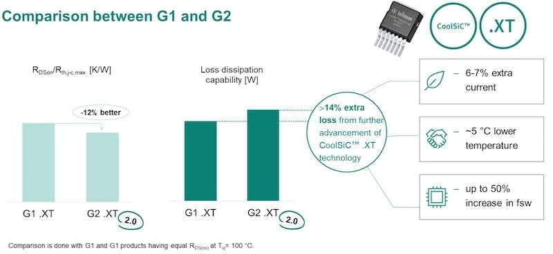
Figure 4
Compared to traditional silicon-based MOSFETs, SiC MOSFETs are renowned for their ability to operate at higher temperatures. Although different SiC MOSFET technologies and manufacturers may have different specific temperature ratings, most SiC MOSFET designs can reliably operate at junction temperatures up to 175C. Infineon's CoolSiC MOSFET 1200 V G2 can operate at temperatures up to 200C for a total cumulative time of 100 hours. The introduction of this equIPMent specification is aimed at improving reliability under overload conditions and providing engineers with greater system design freedom. The ability of SiC MOSFETs to withstand short-term overload is an important consideration in various applications. In industrial motor drives, sudden load changes, additional torque demands, and even power fluctuations can lead to overload situations, in which case higher junction temperature margins are useful. Solar inverters and grid connected applications are other good examples to demonstrate overload situations, as grid voltage fluctuations can affect the operation of power converters. Voltage drop can affect the output power of the converter and temporarily increase power loss. In severe cases, it may even cause the system to be completely disconnected from the power grid. In the application of electric vehicle charging, voltage fluctuations of the charger are crucial. If the input voltage drops, the current may temporarily increase, putting additional pressure on the power device. Figure 5 shows an example of the current capacity expansion of an 8 m Ω device due to higher temperature limitations. The gray curve represents a typical power semiconductor with a junction temperature limit of 175C. In contrast, the green curve of CoolSiC G2 indicates that more current can be achieved at the same operating point (i.e. 150C).
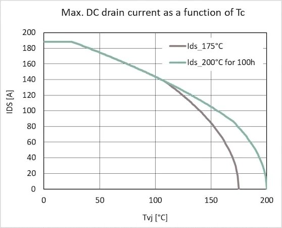
Figure 5
Under the same working conditions, a detailed loss comparison was conducted between the G2 device IMBG120R026M2H and the G1 device IMBG120R030M1H. The conducted loss of the G2 device was reduced by 0.7 W (~3.5%), and the total switching loss was reduced by 5.75 W (~23%). Due to reduced losses and R th, jc is better, and its overall operating junction temperature is also lower.
Shortening dead zone time brings more benefits
Today's MOSFETs can switch within the range of tens of nanoseconds (ns). The switch energy curve provided in the data table shows that by reducing the dead time of the driving voltage in the third quadrant operation (the time when the body diode conducts before the channel opens), the device recovery loss and opening loss can be significantly reduced. The recommended dead time range is between 150 ns and 300 ns. By implementing the suggested value, compared to the nominal device value, the opening loss can be reduced by 20%, and the recovery loss can be reduced by 40%.
The dead time limit depends on various factors, such as parasitic effects in devices and circuits, gate driver speed, and switch current levels. Replacing CoolSiC MOSFET G1 with the most matching G2 device can reduce the required dead time by 30%, as the parasitic capacitance of the switch is improved. This provides greater margin for design, even in the case of simple plug and play MOSFET replacements.
2kV discrete CoolSiC MOSFET
The new 2 kV discrete CoolSiC MOSFET helps to develop more efficient, cost-effective, and simplified energy storage and photovoltaic system designs, meeting the growing demand for higher DC link voltages in these applications.
In order to improve power levels, photovoltaic systems are transitioning towards higher system voltages -1500 V DC is becoming increasingly popular. This transformation aims to reduce power loss and system costs, making renewable energy more affordable.
When designing a solar inverter with a DC link voltage of 1500 V, there are two options. The first option is to use a 3-stage booster as the DC DC maximum power point tracking (MPPT) stage, using a 3-stage topology, such as active neutral point clamping (ANPC) as the DC AC stage. Both levels use 1200 V level equipment to ensure safe and reliable system design. However, this method is relatively more complex and has a larger number of components. The second option is to use a simplified level 2 topology and higher voltage level devices. Based on the performance of the semiconductor devices used, this method may be more efficient. Designers typically choose discrete components to optimize system costs, increase design flexibility, and reduce overall cost of ownership.
At present, the most common discrete semiconductor device in the highest voltage level is the 1700 V device. Although using 1700 V MOSFETs in a 1500 V solar inverter system with a simplified two-level topology seems to be a feasible option, the impact of faults caused by cosmic radiation must be considered. When the blocking voltage exceeds 80% of the rated voltage, these faults will increase sharply. Therefore, using 1700 V MOSFETs in a 1500 V solar inverter system with a 2-level topology will significantly increase its failure rate.
2kV CoolSiC MOSFET
Infineon's new CoolSiC MOSFET 2 kV in a split package can alleviate design challenges and reliability issues. The performance and material list of solar inverters using 2 kV CoolSiC MOSFETs and diodes were compared with inverter designs using 1200 V devices. The system level simulation results show that the loss of the second stage boost stage using CoolSiC 2 kV is 20% lower than that of the third stage boost stage using 1200 V MOSFET. Similarly, the power loss of the 2nd level DC-AC level using CoolSiC 2 kV is 15% lower than that of the 3rd level ANPC level using 1200 V devices. The paper "Performance Evaluation of CoolSiC 2 kV SiC MOSFET Discrete Devices in 1500 V DC Link Systems" in PCIM 2024 will introduce a detailed analysis of simulated and measured data.
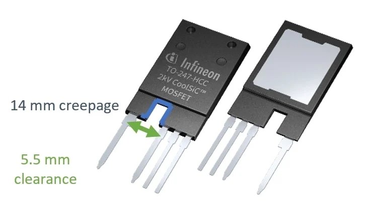
Figure 6
The new CoolSiC 2 kV adopts a new split type TO-247PLUS-4-HCC high creepage distance and gap packaging (as shown in Figure 6), which can ensure the robustness and reliable operation of high-voltage insulation. The product portfolio includes CoolSiC MOSFET 2 kV and Schottky diode 2 kV, with optimized switching performance and high blocking voltage, making it an ideal choice for 1500 V DC systems. The characteristics of the new 2 kV MOSFET make it possible to develop simplified and reliable designs, making it an ideal solution for applications that require high efficiency, low part count, and smaller system size and weight.
High power silicon carbide module
Infineon has launched two models that are sturdy and durable The new 3.3 kV level silicon carbide (SiC) module of XT interconnect technology further enhances the standards in the field of power supply and technology. These modules are designed to provide high power (~1.5 MW) for applications with high task and cycle requirements. These modules include:
FF2000UXTR33T2M1: Room temperature conduction resistance is 1.9 m Ω, nominal current rating is 1000 A
FF2600UXTR33T2M1: Room temperature conduction resistance of 2.5 m Ω, nominal current rating of 750 A
CoolSiC MOSFETs with a rated voltage of 3.3 kV have been optimized to have fast switching and low oscillation trends, thereby reducing total dynamic losses. By using XHP 2 CoolSiC MOSFET in synchronous rectification mode and optimizing the dead time, the total dynamic loss at 150C can be further reduced by about 30%. This means reducing the start and end time of the freewheeling phase, during which the load current is conducted through the integrated diode. CoolSiC MOSFET 3.3 kV adopts a symmetrical design and low inductance (L S=10 nH) XHP 2 packaging, which can fully utilize the potential of fast switching SiC MOSFETs in high voltage and high current applications.
In order to highlight the higher power density that the new SiC power module can provide for traction converters, we compared its performance with that of 3.3 kV IGBT IHV, which is still used in many railway traction converters. Specifically, we compared the performance of a two-stage 3-phase motor inverter based on the 3.3 kV IGBT IHV solution (FZ2400R33H34) with the performance of a two-stage 3-phase motor inverter based on the new 3.3 kV SiC XHP 2 module (two parallel FF2000UXTR33T2M1).
The comparison was conducted under the following conditions: 1800 V DC link voltage (VDC), power factor (pf) 0.9, modulation index (m) 0.9, and 60C coolant temperature (Ta) of the water-cooled radiator. In addition to reducing footprint by nearly 50%, SiC based solutions also reduce total losses by 50%, resulting in a 50% increase in output current at the same switching frequency (1.5 kHz), or an equal output current at four times the high switching frequency (6 kHz instead of 1.5 kHz).
The main characteristics of XHP 2 CoolSiC MOSFET include lower losses, higher switching frequency, and higher power density, which can directly translate into various system advantages. Lower losses help save about 10% of energy at the system level and enable simpler and quieter cooling systems. For example, by using passive motion cooling instead of forced air cooling. Running the converter at a higher switching frequency can reduce motor noise and make magnetic components smaller in size and lighter in weight. A higher power density helps to reduce the volume of the converter by about 10% to 25%. Reducing system volume and weight is crucial, especially in the case of hybrid trains. Here, additional space and reduced weight can be used to increase size, thereby increasing the capacity of the vehicle's traction battery. In addition, lighter system weight and higher efficiency will allow for better utilization of available energy and help achieve the required driving range. Alternatively, if the required driving range has been reached, a lighter system weight and higher efficiency will help optimize and reduce the cost of installing traction batteries, which is still very expensive.
In addition to high output power, many applications such as railway traction and wind power generation also require strong power cycle performance and longer equipment lifespan. Due to the small size of silicon carbide chips and their specific material properties (such as a higher Young's modulus than silicon), using silicon carbide for such applications is more challenging. Under cyclic conditions, these factors can lead to greater thermal mechanical stress on adjacent interconnect layers, thereby reducing the power cycling capability of the module.
Infineon XT technology can compensate for this impact by improving the robustness of the interconnect layer. use. XT's XHP 2 CoolSiC MOSFET 3.3 kV has sturdy copper bonding wires on the copper front metallization layer of SiC chips, sintered chips on the substrate, and highly reliable system solder. This has improved the product's cycling ability and service life, taking SiC power cycling performance to a new level.
To illustrate The powerful features of XT, based on an exemplary task overview of line converters in regional hybrid propulsion trains, are applied to SiC using standard connection technologies (Al bonding lines, Al front metallization of chips, chip solder, system solder) XT's SiC underwent life simulation.
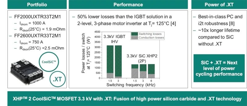
Figure 7
The simulation results indicate that XT has extended the product's lifespan by an order of magnitude - from about 4 years with SiC using standard connection technology to adoption XT's SiC has been around for about 40 years. This indicates that XT is crucial for fully utilizing silicon carbide at higher junction temperatures. To achieve the 30 year service life required for SiC using standard connection technology, it is necessary to significantly reduce the maximum junction temperature during operation.
This means that a larger chip area is required to achieve the required output current. Due to the need for parallel connection at the module level, this can also lead to increased complexity and cost.
In addition to providing first-class circulation capability The advantages of XT for XHP 2 CoolSiC MOSFET also include high surge current tolerance and short circuit withstand time. This provides greater freedom for system designers to handle faults.
Faust Technology focuses on the field of power devices, providing customers with power devices such as IGBT and IPM modules, as well as MCU and touch chips. It is an electronic component supplier and solution provider with core technology.