
 News
News Knowledge Column
Integrating E-mode GaNFET with GaN based gate control circuits can significantly improve the gate drive reliability and compatibility of GaN switches, while maintaining fast switching characteristics and reducing ringing caused by parasitic components related to co packaging.
Development and reliability of cascaded and E-mode GaNFET
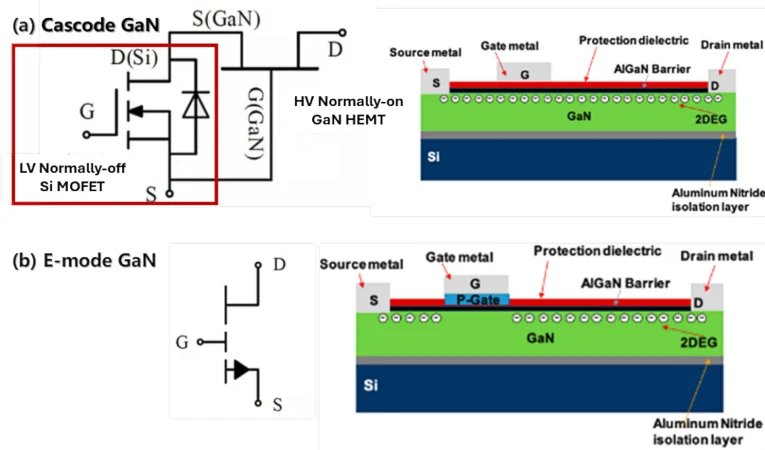
The structure of cascaded GaN (as shown in Figure 1 (a)) combines a low-voltage normally off silicon mosfet and a high-voltage normally on GaN HEMT to form a cascaded configuration. This combination effectively achieves enhanced pattern behavior, and the technology has been commercialized since the early 2010s. The gate threshold voltage of silicon MOSFETs is usually 4 V, which simplifies the gate driving requirements compared to local GaN solutions, as these cascaded GaN can typically be driven by standard silicon gate drivers. In addition, the hybrid characteristics of silicon MOSFETs can enhance reliability. The known characteristics and behavior of silicon can be used to protect the gate of more sensitive GaN HEMTs, reducing the risk of faults caused by high voltage spikes or improper gate voltages.

Figure 1
However, the additional parallel connection of silicon MOSFET between the gate and source of GaN HEMT will significantly increase the effective input capacitance of cascaded GaN devices, which largely sacrifices the fast switching characteristics, which is one of the most prominent advantages compared to SIC MOSFET. Even worse, the series connection of silicon MOSFET and D-mode GaN for co packaging will result in additional parasitic inductance, which can cause more ringing and overshoot in the switching waveform, affecting overall performance and raising concerns about electromagnetic interference (EMI).
The E-mode GaNFET (as shown in Figure 1 (b)) adopts a p-type GaN gate structure, providing a positive threshold voltage, making it naturally normally off in single-chip solutions. This is crucial for power applications that require fail safe operation. E-mode GaNFETs typically exhibit very low gate charge and capacitance without the need for additional components, resulting in faster switching speeds and reduced switching losses. They are highly efficient in applications that require high-frequency operation.
However, the typical gate threshold voltage of p-type GaN gate is 1.4 V, which may cause unexpected device turn-on and system failures due to noise or gate voltage fluctuations. In addition, the typical driving range is -10 V to 7 V, which is incompatible with the driving voltage of most other power devices (requiring 12-18 V), making it difficult to switch from other power switches to GaN HEMTs. Finally, due to the immaturity and fragility of p-type GaN gates, there are concerns about long-term reliability and threshold voltage stability.
Full GaN Integrated Circuit Solution: Leap in Gate Threshold Voltage and Driving Range
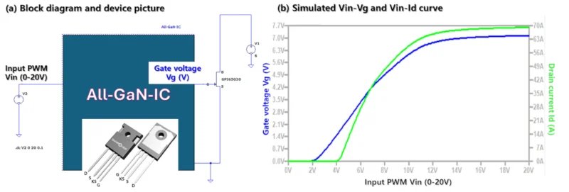
GaNPower International has innovated a fully GaN integrated circuit method, increasing the gate threshold voltage from 1.4 V to an impressive 3.5-4.0 V and expanding the driving range to 20 V. A proprietary GaN based gate adjustment circuit has been integrated with the power GaNFET single-chip. As shown in Figure 2 (a), this innovation matches the pin arrangement, threshold voltage, and driving range of the new E-mode GaN with silicon and SiC MOSFETs, making it known as "pin to pin" (P2P) with excellent compatibility. P2P technology combines the advantages of cascaded GaN and E-mode GaN, aiming to achieve more reliable gate driving without significantly sacrificing the fast switching advantage of GaN power switch.
According to the LTSpice simulation results shown in Figure 2 (b), the gate threshold voltage of the P2P GaN switch has been raised to about 4 V, and its gate voltage is effectively clamped below 7 V under 0-20 V PWM input.

Figure 2
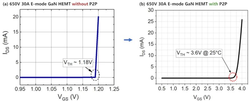
The static IdVg measurement results at room temperature (as shown in Figure 3) also confirmed the improvement of the gate threshold voltage (3.6 V) of P2P GaN compared to normal E-mode GaN without GaN based gate adjustment circuit.

Figure 3
Showcasing excellent switch performance
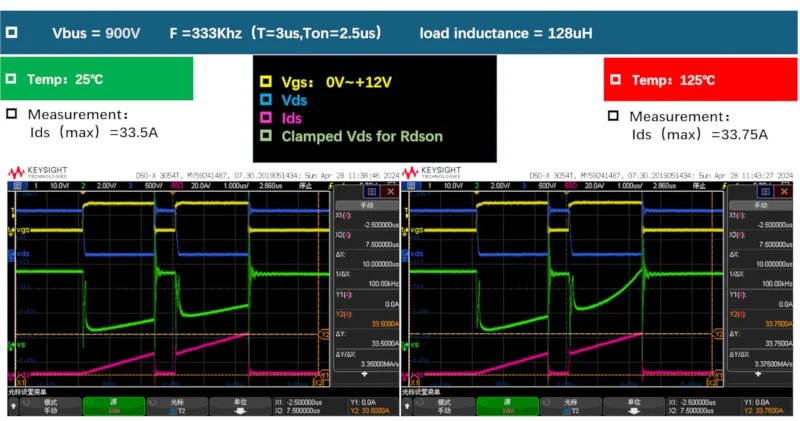
A dual pulse testing platform has been established, equipped with customized air core 128 μ H load inductors, freely rotating SiC diodes, and reliable voltage clamp circuits to accurately measure dynamic Rdson and evaluate the burst mode switching performance of P2P GaN.
At a 12V PWM input and a 900V bus voltage, all switch waveforms (Vgs, Vds, and Ids, as shown in Figure 4) are clean without obvious ringing or overshoot. In addition, the dynamic Rdson remains within a reasonable range at room temperature, with a maximum current rating of 33 A, which can be observed from the clamped Vds waveform. Another dual pulse test conducted under similar loading conditions at 125C showed comparable switching waveforms, demonstrating the good thermal stability of GaN based gate control circuits.

Figure 4
A 100 KHz half bridge Buck testing platform was established for continuous hard switching evaluation of P2P GaN, equipped with a high saturation ring power inductor and a 40 ohm high-power resistive load. Two GP65R45T4 devices were installed on the main test board with suitable heat sinks, and appropriate fans were used for cooling during testing.
According to the efficiency report shown in Figure 5 (a), the P2P GaN based Buck converter achieved a peak efficiency of 97.42% and a maximum power output of 3.7 kW at a 12 V PWM input and a bus voltage of 200-550 V. Figure 5 (b) shows the good continuity of the switch waveform at peak efficiency under a bus voltage of 450 V, without significant ringing or overshoot.

Figure 5
Fushite Technology focuses on the field of power devices, providing customers with power devices such as IGBT and IPM modules, as well as MCU and touch chips. It is an electronic component supplier and solution provider with core technology.