
 News
News Knowledge Column
Gallium nitride (GaN) high electron mobility transistor (HEMT) power devices have many advantages in fast switching power conversion applications and have been widely used in mobile phone/laptop power adapters/chargers, data center power supplies, and renewable energy systems. In this article, we delve into a novel application created by Innoscience for battery management systems (BMS) that utilizes GaN HEMTs designed as bidirectional devices.
The advantages of bidirectional switches and GaN HEMTs
Bidirectional switches (BDSes) have many different applications, one example of which is AC/AC ring converters, which can replace AC/DC+DC/AC stages in solar inverters. Bidirectional operation enables four quadrant switching, reducing the number of components and improving efficiency, power density, and reliability. Silicon mosfet has an intrinSIC body diode that conducts in reverse mode (i.e. for NMOS devices, when the drain is at a negative potential relative to the source). However, the reverse operation of MOSFETs has very limited gate control. Therefore, two back-to-back MOSFETs are usually used in series. Current flows through the MOSFET of one device and the body diode of another device. The sum of the conduction losses of two devices in either direction.
GaN HEMT is a lateral device without a body diode. Therefore, bidirectional current flow can be easily achieved in a single device. The voltage blocking capability is usually achieved by creating a lateral drift region at the drain. Processing the source side of the channel in a similar manner to create symmetrical devices can achieve bidirectional voltage blocking capability. Compared with silicon MOSFETs, some advantages of this method are as follows:
A GaN device can replace two MOSFETs.
The material advantages of GaN, as well as the high carrier mobility and saturation velocity achieved in the two-dimensional electron gas channel of HEMTs, have improved the specific on state resistance (RDS (on) area) index. This translates into lower conduction losses. In applications that require high-frequency switching, the lower parasitic capacitance of GaN significantly improves the switching quality factor and reduces losses.
The threshold voltage (Vth) of silicon MOSFETs typically has a negative temperature coefficient, resulting in a positive temperature coefficient (PTC) of the drain current (or an increase in conduction under a given gate drive), until the zero temperature coefficient point in the drain current characteristics. After this point, as the temperature increases, mobility decreases and the current decreases. The PTC region of drain current may increase the risk of thermal runaway, especially at higher drain biases, and limit the safe operating region (SOA) of the device below theoretical limits. This is called the Spirito effect. Due to the highly stable Vth characteristics of GaN HEMTs at different temperatures, they exhibit minimal Spirito effect compared to silicon MOSFETs, resulting in stable SOA over a temperature range.
VGaN devices in BMS
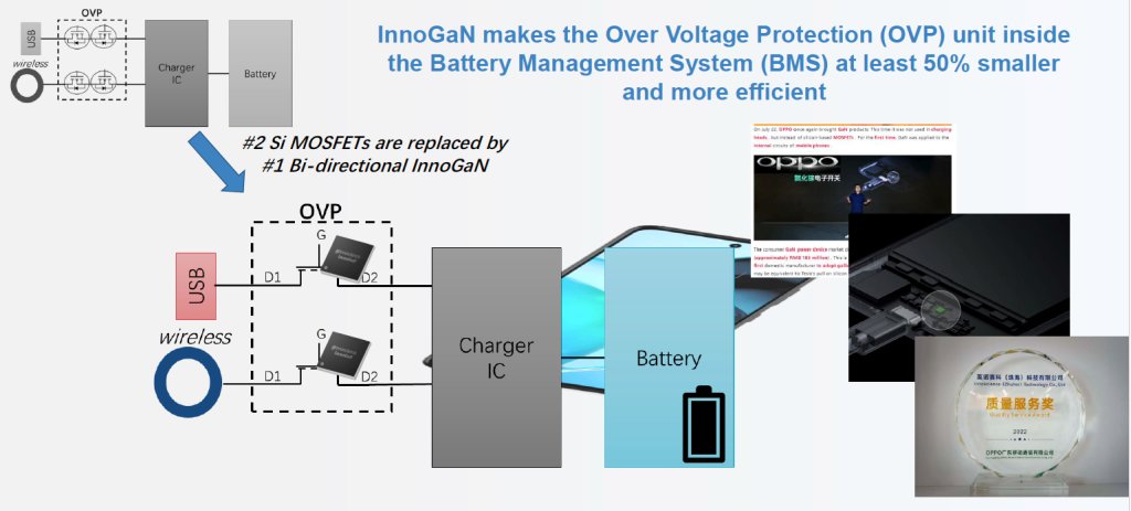
Innoscience has utilized the advantages of GaN HEMTs mentioned above to create a bidirectional device called VGaN. The main application goal of this device is to serve as an overvoltage protection (OVP) load switch in BMS. Taking the laptop battery charging system as an example. Modern laptops can be charged through USB ports or wireless methods. Laptops require bidirectional functionality, such as providing charging power for mobile phones. The OVP circuit required for each charging channel requires at least four silicon MOSFETs to achieve bidirectionality. It can be completed using two GaN BDS devices. Some requirements for BDS devices in this application are:
Low conduction loss. BDS is usually turned on and only turned off when the system detects overvoltage. Therefore, low RDS (on) is an important consideration factor.
Small footprint. Mobile devices are typically limited by space and weight.
Low standby leakage. This reduces the burden that these devices may cause on the battery when not charging.
Low cost: This is a key requirement in any consumer electronic device.
Innoscience has launched a series of VGaN devices with voltage levels ranging from 40 V to 100 V. 40-V devices can be used, for example, for smartphone battery OVP applications. The 40-V product line features VGaN devices with RDS (on) ranging from 1.2 m Ω to 12 m Ω. INN040W048A is a 4.8-m Ω, 20-A VGaN device packaged in a small WLCSP 2.1 2.1-mm. As an example of OVP in commercial applications, it is showcased in the application announcement of the OnePlus 11R smartphone, as shown in Figure 1. This follows the use of VGaN devices in other phones such as OPPO Reno7 Pro and RealMe GT2 Master Edition. VGaN achieves a space saving of 64% and also reduces peak power heating by 85% during charging.

Figure 1
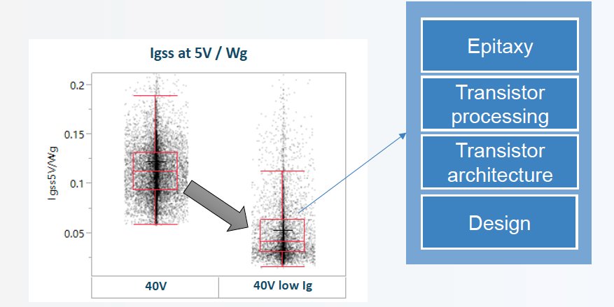
Low standby leakage is a key indicator of OVP devices, and Innoscience has modified the standard unidirectional HEMT process and design to meet this requirement in its VGaN devices. As shown in Figure 2, the combination of epitaxy and design modifications can reduce gate leakage. The maximum 5-V gate to drain leakage specification for INN040W048A at 85C temperature is 3 µ A.

Figure 2
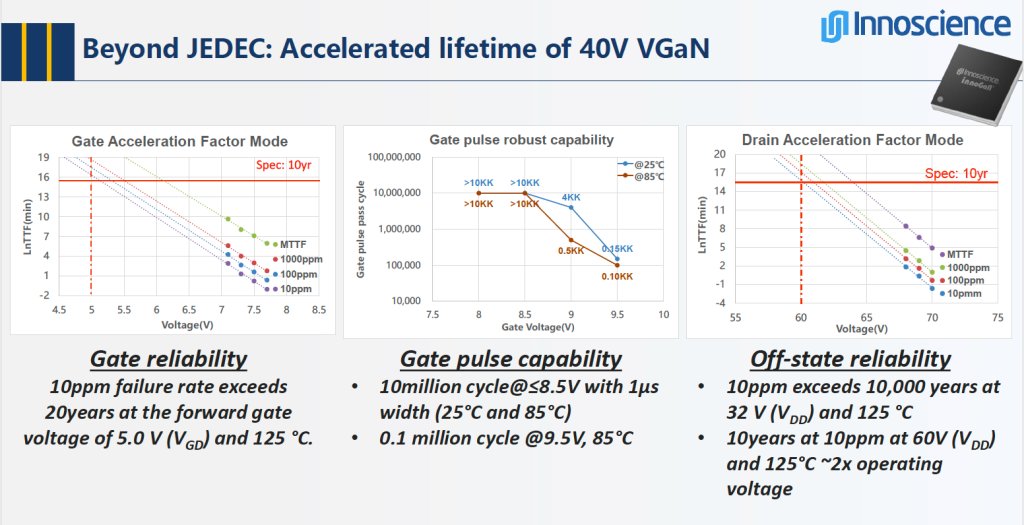
VGaN products such as INN040W048A have undergone a complete JEDEC reliability testing suite. Tests requiring high drain bias, such as standard high temperature reverse bias (HTRB) and its high humidity version (H3TRB), are conducted on two drain nodes with a 32-V drain bias to ensure reliable bidirectional blocking. In addition, an accelerated lifespan test was conducted, as shown in Figure 3. These tests indicate that the gate failure rate at 10 ppm exceeds 20 years at 5 V and 125C. The reliability study of accelerating high drain bias shutdown state has calculated that the 10 ppm failure rate lifespan under 32-V drain bias exceeds 10000 years.

Figure 3
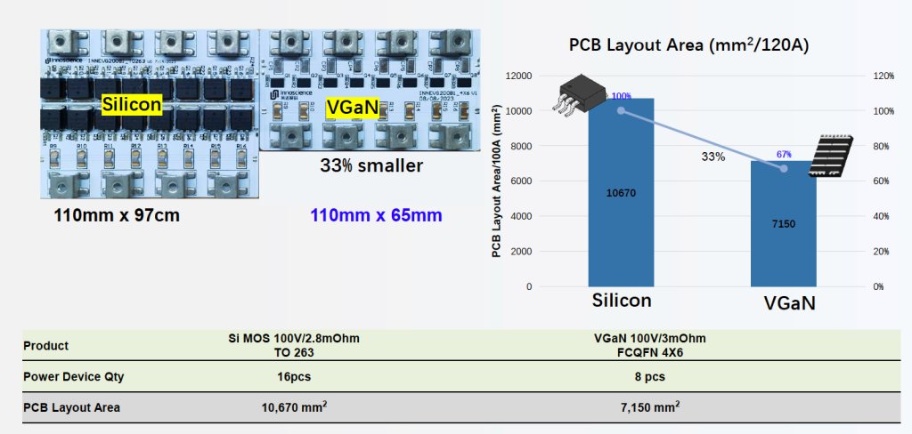
Innoscience also produces 100-V VGaN devices, targeting many 48-V battery applications, including electric bicycles and energy storage systems. INN100FQ030A is a 100-V, 3.2-m Ω BDS, packaged in FCQFN 4 6-mm. Figure 4 shows the size advantage of this device compared to using a 100-V silicon MOSFET. Tests conducted at a current of 100 A showed that compared to silicon MOSFETs, the junction temperature increase of VGaN was much smaller, only 4.7C, while that of silicon MOSFETs was 11C. This is attributed to the stable Vth of GaN devices and their decreasing transconductance with temperature variation.

Figure 4
Innoscience has created a 48-V/180-A BMS high side demonstration board. It uses 16 parallel INV100FQ030A devices to provide charging and discharging same port battery protection. No external heat sink is required, and the maximum temperature rise is maintained at or below 50C. Applications include electric two wheelers and energy storage systems.
VGaN devices utilize the advantages of GaN HEMTs for novel applications, such as OVP in BMS. The use of VGaN devices in smartphones and other mobile devices also utilizes the high production capacity of its 8-inch GaN on silicon factory. The advantages of VGaN make it suitable for many other applications that require batteries, such as energy storage systems and two wheeled vehicles.
Fushite Technology focuses on the field of power devices, providing customers with power devices such as IGBT and IPM modules, as well as MCU and touch chips. It is an electronic component supplier and solution provider with core technology.